BA6427F データシートの表示(PDF) - ROHM Semiconductor
部品番号
コンポーネント説明
一致するリスト
BA6427F Datasheet PDF : 5 Pages
| |||
Motor driver ICs
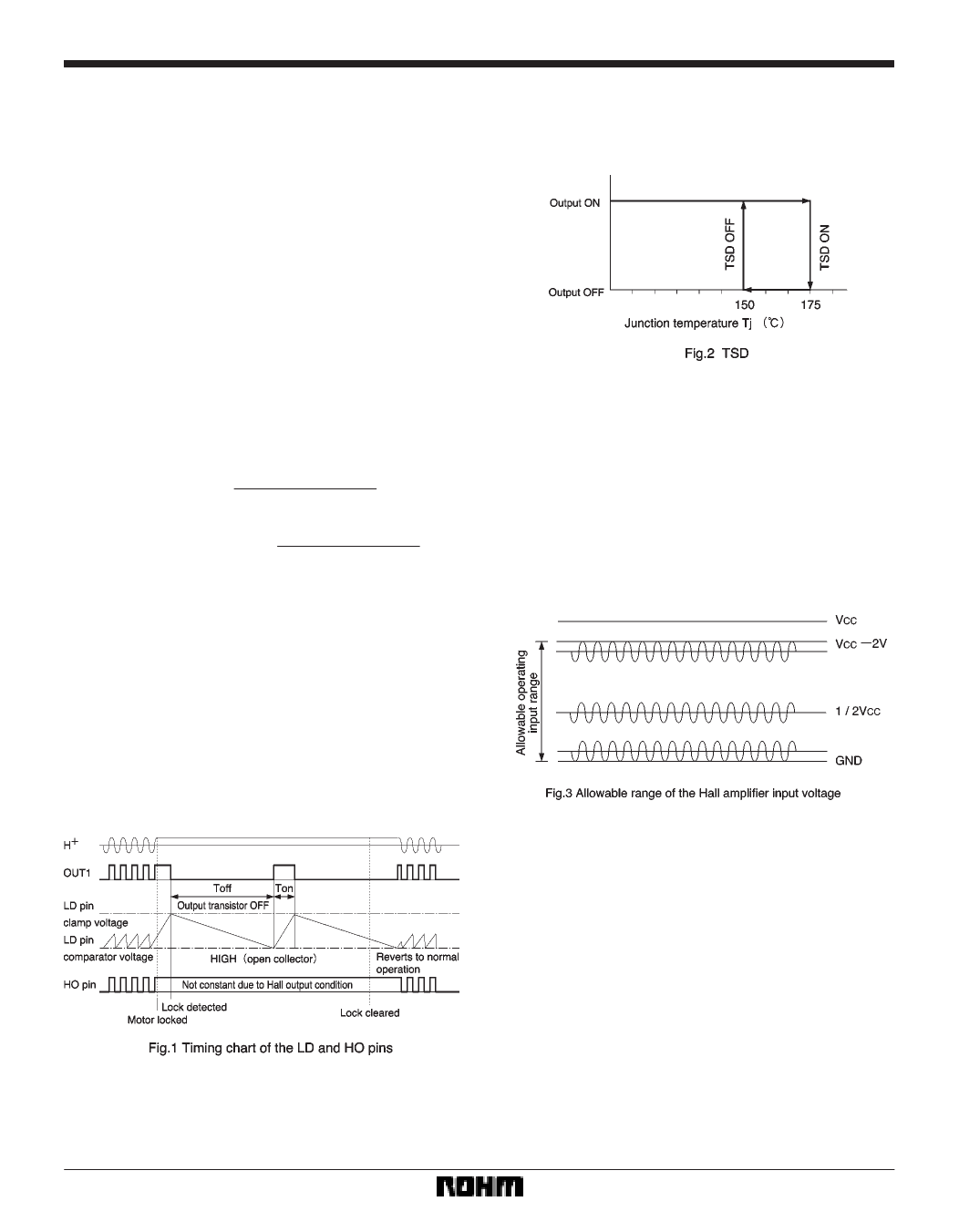
FLock detection
The automatic restart circuit detects a motor lock condi-
tion and automatically turns off the output power. When
the lock condition is cleared, the IC automatically restarts
and allow the motor to run.
In the BA6427F, automatic restart is performed as fol-
lows.
A motor lock condition is detected when the Hall signal
stops switching. The output is OFF when the LD pin is be-
ing charged.
(1) The HO pin outputs a signal synchronized with the
Hall signal.
(2) The HO pin is an open collector output.
The time required for the external capacitor at the LD pin
to charge or discharge when the motor is locked varies
with the capacitor size. The charge and discharge times
are obtained by:
C (VLDCL – VLDCP)
TON (charge time) =
ILDC
TOFF (discharge time) =
C (VLDCL – VLDCP)
ILDD
C is the capacitance of the external capacitor connected
to the LD pin,
VLDCL is the LD pin clamp voltage
(1.93V Typ.),
VLDCP is the LD pin comparator voltage (0.76V Typ.),
ILDC is the LD pin charge current
(2.9µA Typ.),
ILDD is the LD pin discharge current
(0.48µA Typ.).
For C = 0.47µF, for example, the charge and discharge
times are 0.19 s (output ON) and 1.15 s (output OFF),
respectively.
The timing of the LD pin is shown in Fig.1.
766
BA6427F
FOperation notes
(1) Thermal shutdown circuit
The IC has a built-in thermal shutdown circuit. There is
a degree of hysteresis in the TSD circuit.
The circuit is activated at the temperature of about 175_C
(typical), so that all outputs are turned OFF. The circuit is
deactivated when the temperature drops to about
150_C, and normal operation resumes. (With the typical
values, there is a hysteresis of 25_C.)
(2) Current consumption
The power dissipated by the IC varies widely with the
supply voltage and the output current. Make sure that
your application does not exceed the allowable power
dissipation of the IC package.
(3) Hall input pins (H), H*)
(1) The values of the Hall device bias resistors (see the
block diagram) must be set so as to maintain the Hall am-
plifier input bias voltage within the range of 0V to VCC-2V,
including the signal amplitude. It is recommended that
the same value be used for both resistors so that the Hall
device output signal centered around VCC / 2 is input to
the IC.
(2) Be careful of the input signal for the Hall inputs of this
IC have no hysteresis.
(4) ASO
Make sure that the output current will not exceed the ab-
solute maximum rating or the ASO value.
(5) Ground pin potential
Be sure to keep the GND potential lower than the poten-
tials of the other pins.
Share Link: 