LTC1262 データシートの表示(PDF) - Linear Technology
部品番号
コンポーネント説明
一致するリスト
LTC1262 Datasheet PDF : 8 Pages
| |||
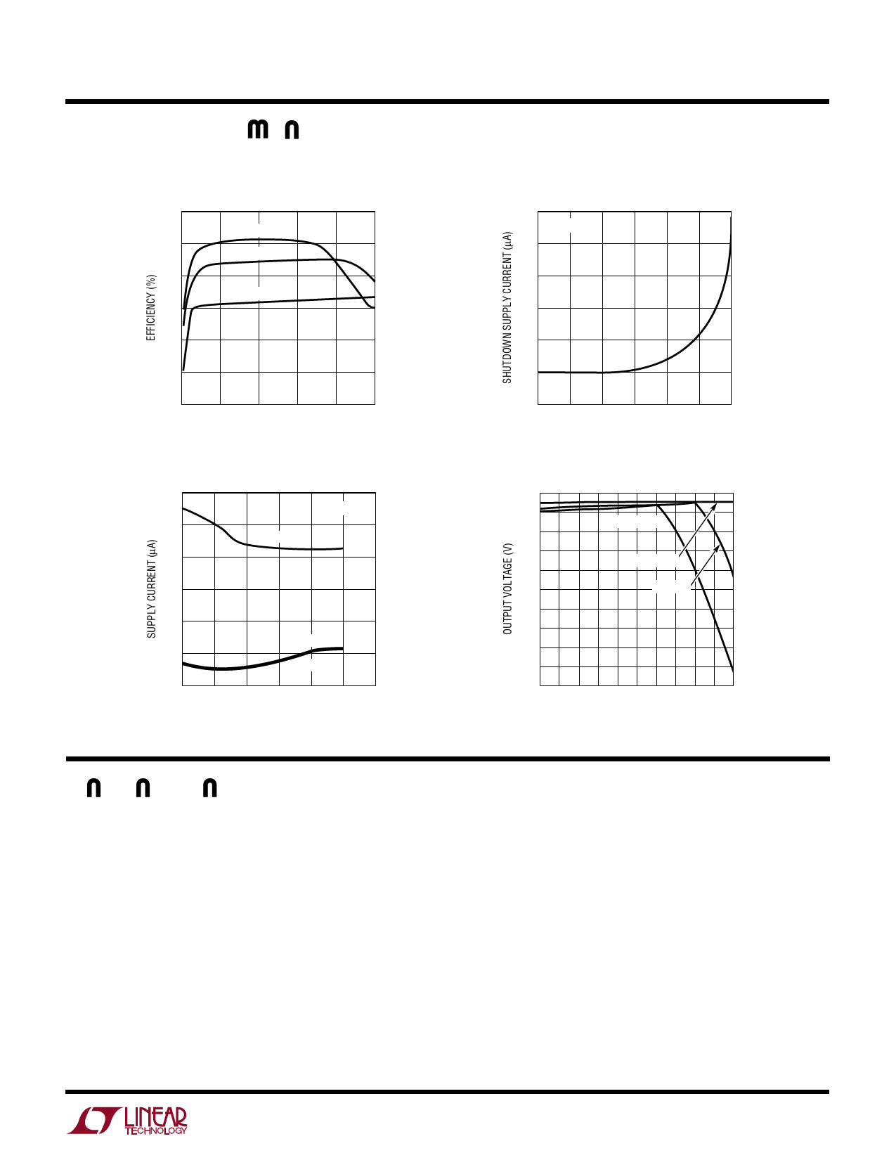
TYPICAL PERFORMANCE CHARACTERISTICS
LTC1262
Efficiency vs Output Current
85
VCC = 4.75V
80
VCC = 5V
75
VCC = 5.5V
70
65
60
55
0
10
20
30
40
50
OUTPUT CURRENT (mA)
LTC1262 G01
Supply Current vs Supply Voltage
600
IOUT = 0
580
TA = 70°C
560
540
520
500
480
4.5
TA = 25°C
TA = 0°C
4.75 5.0 5.25 5.5 5.75 6.0
SUPPLY VOLTAGE (V)
LTC1262 G03
Shutdown Supply Current
vs Temperature
3.6
VCC = 5V
3.0
2.4
1.8
1.2
0.6
0
–50 –25 0
25 50
TEMPERATURE (°C)
75 100
LTC1262 G02
Output Voltage vs Output Current
12.2
12.0
VCC = 4.75V
11.8
11.6
VCC = 5.5V
11.4
11.2
VCC = 5V
11.0
10.8
10.6
10.4
10.2
0 5 10 15 20 25 30 35 40 45 50
OUTPUT CURRENT (mA)
1262 G04
PI FU CTIO S
C1– (Pin 1): C1 Negative Input. Connect a 0.22µF capaci-
tor C1 between C1+ and C1–.
C1+ (Pin 2): C1 Positive Input. Connect a 0.22µF capaci-
tor C1 between C1+ and C1–.
C2 – (Pin 3): C2 Negative Input. Connect a 0.22µF capaci-
tor C2 between C2+ and C2 –.
C2+ (Pin 4): C2 Positive Input. Connect a 0.22µF capaci-
tor C2 between C2+ and C2 –.
VCC (Pin 5): Positive Supply Input Where 4.75V ≤ VCC
≤ 5.5V. Connect a 4.7µF bypass capacitor CIN to ground.
VOUT (Pin 6): 12V Output. Connect a 4.7µF bypass capaci-
tor COUT to ground. When in the shutdown mode VOUT =
VCC.
GND (Pin 7): Ground.
SHDN (Pin 8): Logic Level Shutdown Pin. Application of a
logic low at SHDN pin will place the regulator in normal
operation. With no external connection, or with SHDN tied
to VCC, the device will be put into shutdown mode. Connect
to GND for normal operation. In shutdown mode the
charge pump is turned off and VOUT = VCC.
3
Share Link: 