PS398 データシートの表示(PDF) - Pericom Semiconductor
部品番号
コンポーネント説明
一致するリスト
PS398 Datasheet PDF : 10 Pages
| |||
PS398/PS399
1122334455667788990011223344556677889900112233445566778899001122112233445566778899001122334455667788990011223344556677889900112211223344556677889900112233445566778899001122334455667788990011221122334455667788990011223344556677889900112233445566778899001122112233445566778899001122
Precision 8-Ch, Diff. 4-Ch,
17V Analog Multiplexers
Features
Description
• Low On-Resistance (60Ω typ.) Minimizes Distortion
and Error Voltages
• Low Glitching Reduces Step Errors and Improves
Settling Times. Charge Injection: <5pC
• Split-Supply Operation (+3V to +8V)
• Improved Second Sources for MAX398/MAX399
• On-Resistance Matching Between Channels: <6Ω
• On-Resistance Flatness: <11Ω
• Low Off-Channel Leakage,
INO(OFF) < 1nA @ +85oC, ICOM(ON), <2.5nA @ +85oC
• TTL/CMOS Logic Compatible
• Fast Switching Speed, tTRANS <250ns
• Break-Before-Make action eliminates momentary crosstalk
• Rail-to-Rail Analog Signal Range
• Low Power Consumption, <300µW
• Narrow SOIC and QSOP Packages Minimize Board Area
Applications
• Data Acquisition Systems
• Audio Switching and Routing
• Test Equipment
• PBX, PABX
• Telecommunication Systems
• Battery-Powered Systems
The PS398/PS399 are improved high precision analog multiplex-
ers. The PS398, an 8-channel single-ended mux, selects one of
eight inputs to a common output as determined by a 3-bit address
A0-A2. An EN (enable) pin when low disables all switches, use-
ful when stacking several devices. The PS399 is a 4-channel
differential multiplexer. It selects one of four differential inputs to
a common differential output as determined by a 2-bit address A0,
A1. An EN pin may be driven low to disable all switches.
These multiplexers operate with dual supplies from +3V to +8V.
Single-supply operation is possible from +3V to +15V.
With +5V power supplies, the PS398/PS399 guarantee <100Ω
on-resistance. On-resistance matching between channels is within
6Ω. On-resistance flatness is less than 11Ω over the specified
signal range.
Each switch conducts current equally well in either direction when
on. In the off state each switch blocks voltages up to the power-
supply rails.
Both devices guarantee low leakage currents (<2.5nA at +85oC)
and fast switching speeds (tTRANS <250ns). Break-before-make
switching action protects against momentary crosstalk between
channels.
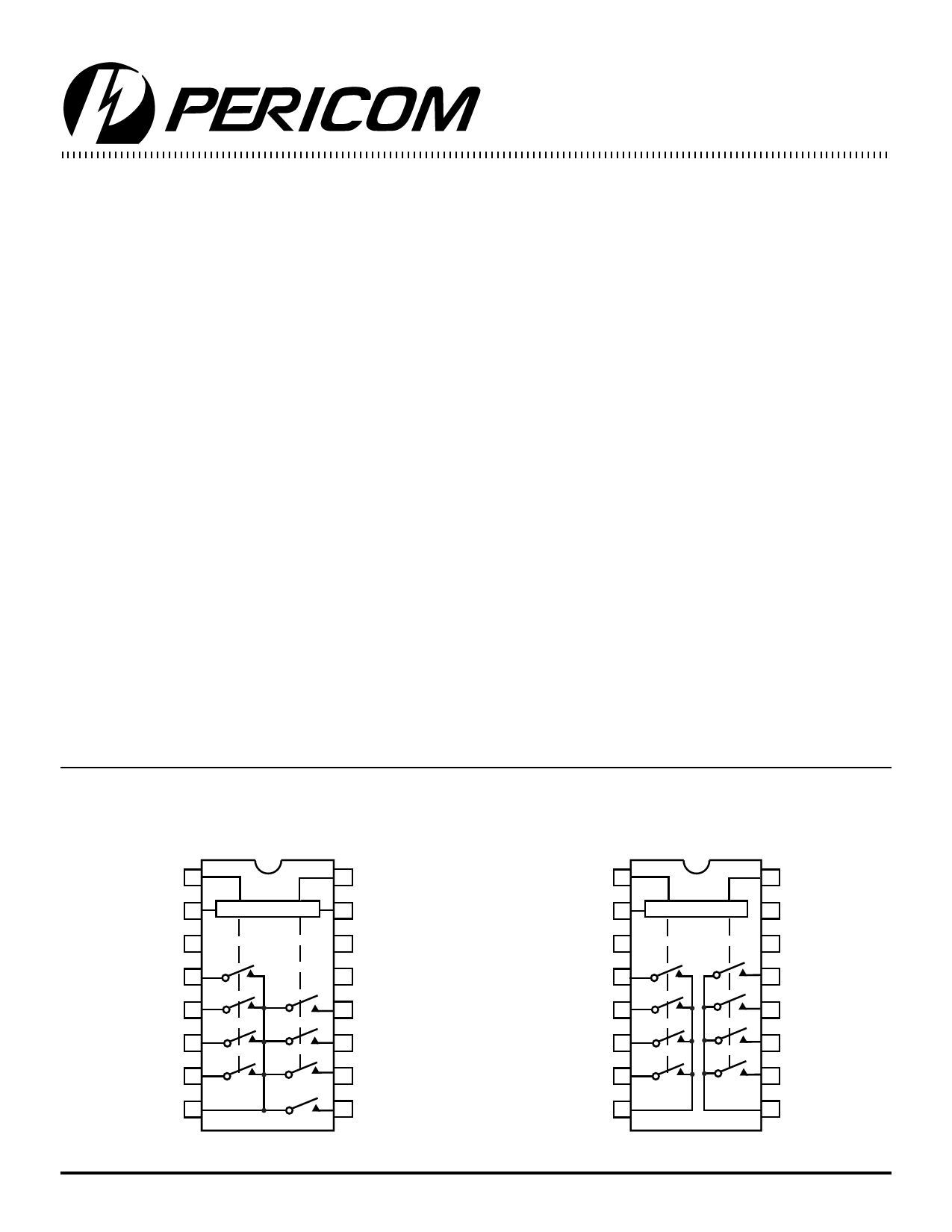
Functional Block Diagrams and Pin Configurations
Top View
PS398
Top View
PS399
A0 1
16 A1
EN 2 Decoders/Drivers 15 A2
V- 3
14 GND
NO1 4
13 V+
NO2 5
12 NO5
NO3 6
11 NO6
NO4 7
10 NO7
COM 8
9 NO8
AO 1
16 A1
EN 2 Decoders/Drivers 15 GND
V- 3
14 V+
NO1A 4
13 NO1B
NO2A 5
12 NO2B
NO3A 6
11 NO3B
NO4A 7
10 NO4B
COMA 8
9 COMB
1
PS8185C 10/06/99
Share Link: 