HIP1011(1999) データシートの表示(PDF) - Intersil
部品番号
コンポーネント説明
一致するリスト
HIP1011 Datasheet PDF : 7 Pages
| |||

HIP1011
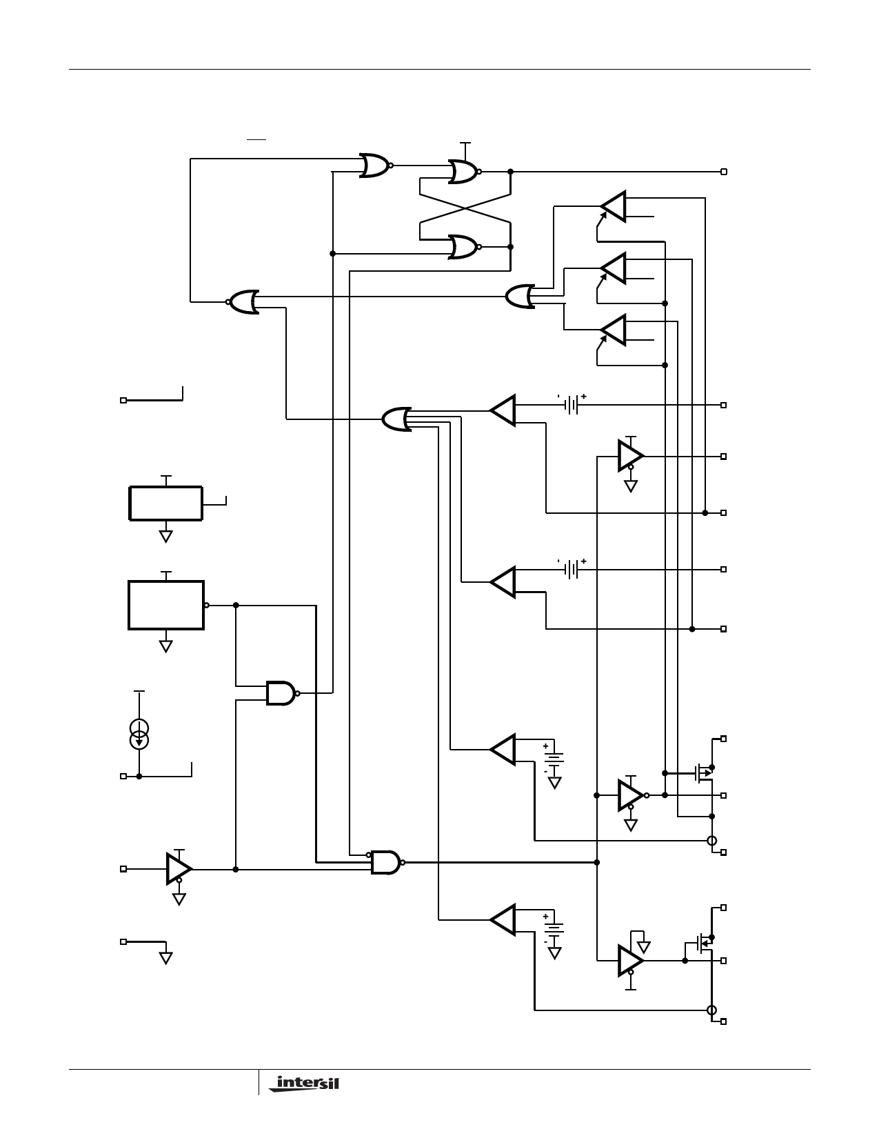
Pin Descriptions
PIN DESIGNATOR
FUNCTION
DESCRIPTION
1
M12VIN
-12V Input
-12V Supply Input. Also provides power to the -12V overcurrent circuitry.
2
FLTN
Fault Output
5V CMOS Fault Output; LOW = FAULT. An optional capacitor may be place from this pin to
ground to provide additional immunity from power supply glitches.
3
3V5VG
3.3V/5V Gate Output Drive the gates of the 3.3V and 5V MOSFETs. Connect a capacitor to ground to set the start-
up ramp. During turn on, this capacitor is charged with a 25µA current source.
4
VCC
12V VCC Input Connect to unswitched 12V supply.
5
12VIN
12V Input
Switched 12V supply input.
6
3VISEN
3.3V Current Sense Connect to the load side of the current sense resistor in series with source of external 3.3V
MOSFET.
7
3VS
3.3V Source
Connect to source of 3.3V MOSFET. This connection along with pin 6 (3VISEN) senses the
voltage drop across the sense resistor.
8
OCSET
Overcurrent Set Connect a resistor from this pin to ground to set the overcurrent trip point of all four switches. All
four over current trips can be programmed by changing the value of this resistor. The default
(6.04kΩ, 1%) is compatible with the maximum allowable currents as outlined in the PCI specifi-
cation.
9
PWRON
Power On Control Controls all four switches. High to Turn Switches ON, Low to turn them OFF.
10
5VS
5V Source
Connect to source of 5V MOSFET switch. This connection along with pin 11(5VISEN) senses
the voltage drop across the sense resistor.
11
5VISEN
5V Current Sense Connect to the load side of the current sense resistor in series with source of external 5V MOSFET.
12
12VO
Switched 12V Output Switched 12V output.
13
GND
Ground
Connect to common of power supplies.
14
12VG
Gate of Internal Connect a capacitor between 12VG and 12VO to set the start up ramp for the +12V supply.
PMOS
This capacitor is charged with a 25µA current source during start -up. The 3.3V and 5V UV
circuitry is enabled after the voltage on 12VG is less than 400mV. Therefore, if the capacitor
on the pin 3 (3V5VG) is more than 25% larger than the capacitor on pin 14 (12VG) a false UV
may be detected during start up.
15
M12VG
Gate of Internal Connect a capacitor between M12VG and M12VO to set the start up ramp for the M12V supply.
NMOS
This capacitor is charged with 25µA during start up.
16
M12VO
Switched -12V
Output
Switched 12V Output.
2-3