AV9154A-60 データシートの表示(PDF) - Integrated Circuit Systems
部品番号
コンポーネント説明
一致するリスト
AV9154A-60 Datasheet PDF : 7 Pages
| |||
AV9154A-60
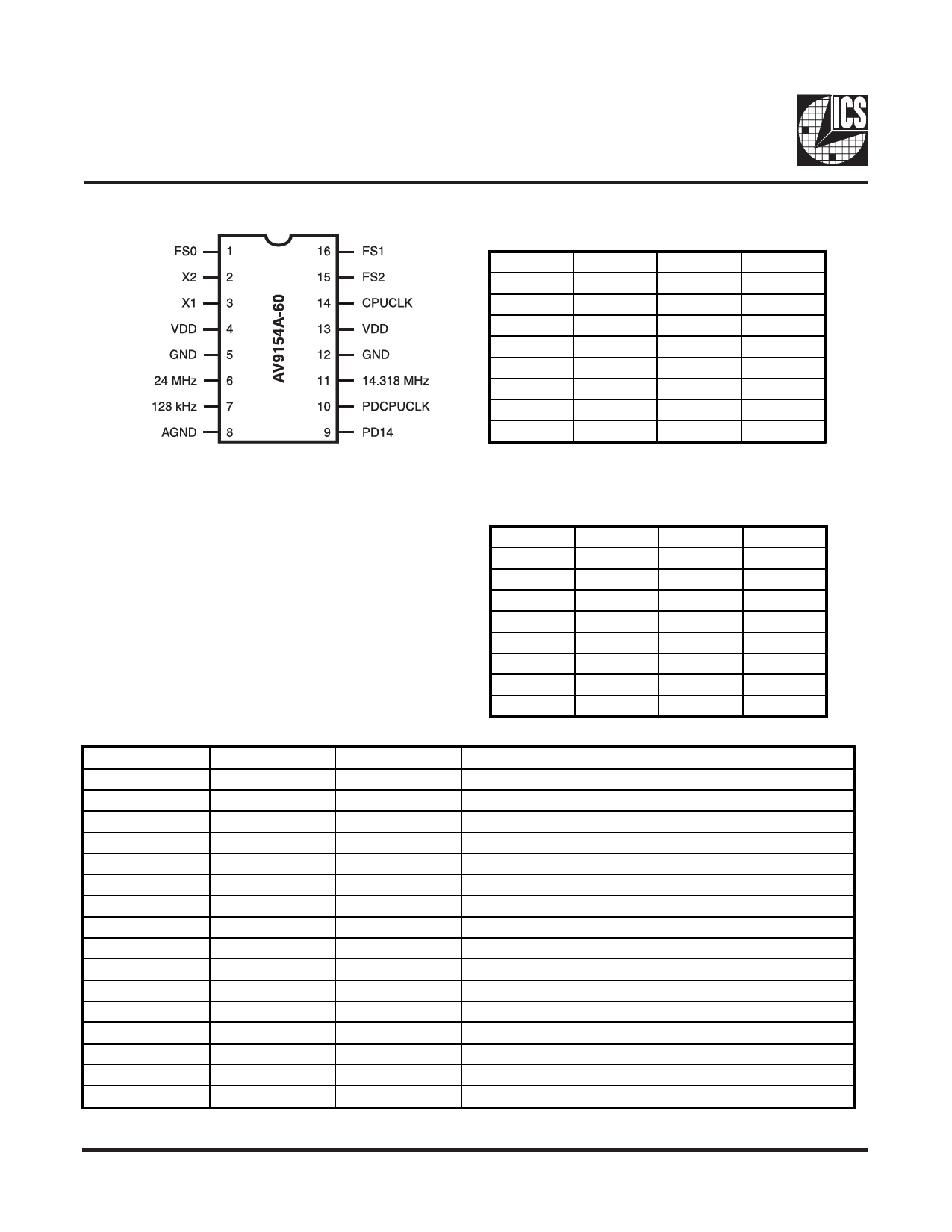
Pin Configuration
16-Pin SOIC
Pin Descriptions
PIN NUMBER
1
2
3
4
5
6
7
8
9
10
11
12
13
14
15
16
PIN NAME
FS0
X2
X1
VDD
GND
24 Mhz
128 kHz
AGND
PD14
PDCPUCLK
14.318 Mhz
GND
VDD
CPUCLK
FS2
FS1
Note:
No internal pull-ups on any Inputs.
* Frequencies shown are assuming a 14.318 MHz input.
TYPE
I
O
I
P
P
O
O
P
I
I
O
P
P
O
I
I
Functionality
(in MHz, assuming 14.318 MHz input)
FS2
FS1
FS0
CPUCLK
0
0
0
8
0
0
1
16
0
1
0
20
0
1
1
25
1
0
0
33.33
1
0
1
40
1
1
0
50
1
1
1
66.66
Actual Output Frequencies
(in MHz, assuming 14.318 MHz input)
FS2
FS1
FS0
CPUCLK
0
0
0
8.182
0
0
1
16.11
0
1
0
20.05
0
1
1
25.06
1
0
0
33.24
1
0
1
40.09
1
1
0
50.11
1
1
1
66.48
DESCRIPTION
Frequency Select 0 for CPUCLK.
Crystal out. Connect a 14.318 MHz crystal to this pin.
Crystal in. Connect a 14.318 MHz crystal to this pin.
Digital Power (+3.3V or +5V).
Digital Ground.
24 MHz clock output.*
128 kHz clock output.*
Analog Ground.
Power-down 14.318 MHz output (active high).
Power-down CPU clock (active high).
14.318 MHz reference clock output.*
Digital Ground.
Digital Power (+3.3V or +5V).
CPU Clock output determined by status of FS0 - FS2.
Frequency Select 2 for CPUCLK.
Frequency Select 1 for CPUCLK.
2
Share Link: 