SL74HC374 データシートの表示(PDF) - System Logic Semiconductor
部品番号
コンポーネント説明
一致するリスト
SL74HC374
System Logic Semiconductor

SL74HC374 Datasheet PDF : 5 Pages
| |||
SL74HC374
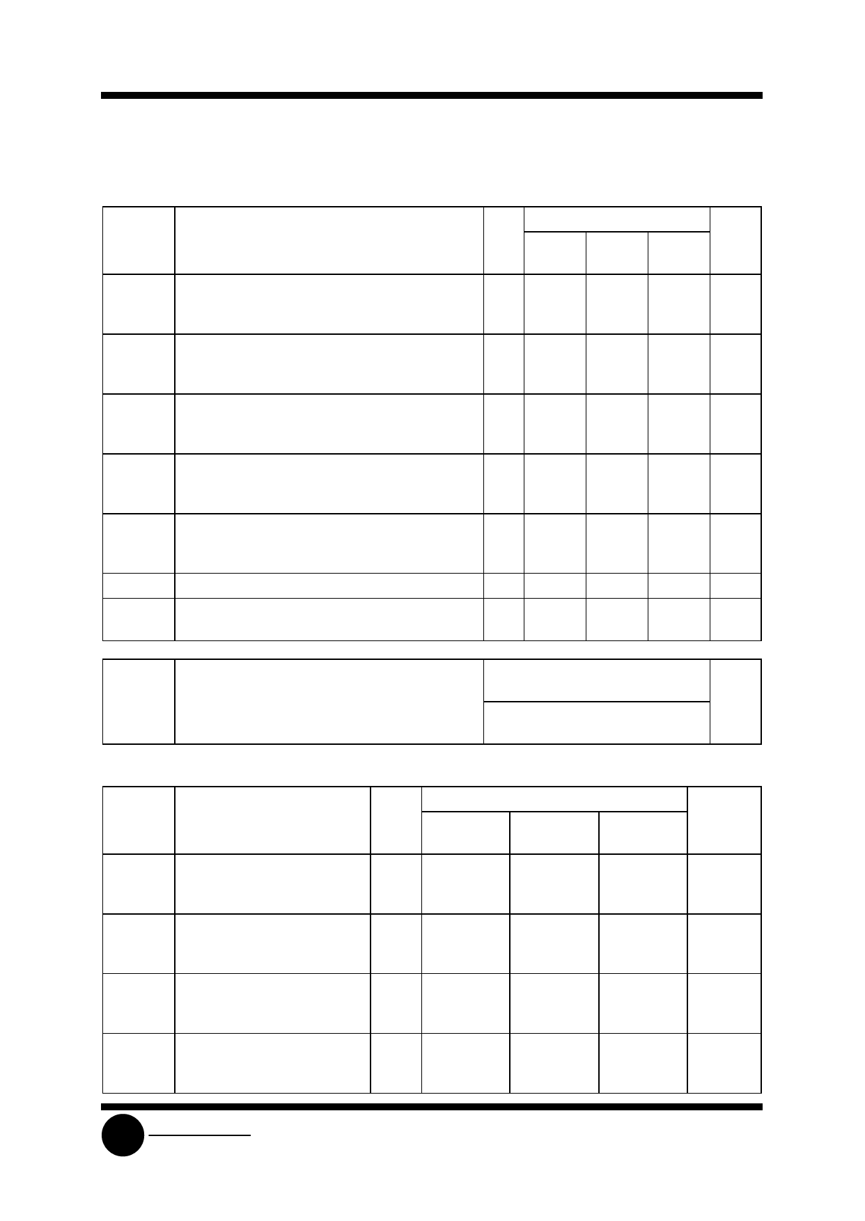
AC ELECTRICAL CHARACTERISTICS(CL=50pF,Input tr=tf=6.0 ns)
Symbol
Parameter
fmax Maximum Clock Frequency (50% Duty Cycle)
(Figures 1 and 4)
tPLH, tPHL Maximum Propagation Delay, Clock to Q (Figures
1 and 4)
tPLZ, tPHZ Maximum Propagation Delay, Output Enable to Q
(Figures 2 and 5)
tPZH, tPZL Maximum Propagation Delay, Output Enable to Q
(Figures 2 and 5)
tTLH, tTHL Maximum Output Transition Time, Any Output
(Figures 1 and 4)
CIN
Maximum Input Capacitance
COUT Maximum Three-State Output Capacitance
(Output in High-Impedance State)
VCC
Guaranteed Limit
V 25 °C to ≤85°C ≤125°C Unit
-55°C
2.0 6.0
5.0
4.0 MHz
4.5 30
24
20
6.0 35
28
24
2.0 125
155
190
ns
4.5 25
31
38
6.0 21
26
32
2.0 150
190
225
ns
4.5 30
38
45
6.0 26
33
38
2.0 150
190
225
ns
4.5 30
38
45
6.0 26
33
38
2.0 75
95
110
ns
4.5 15
19
22
6.0 13
16
19
-
10
10
10
pF
-
15
15
15
pF
Power Dissipation Capacitance (Per Enabled
Output)
CPD Used to determine the no-load dynamic power
consumption: PD=CPDVCC2f+ICCVCC
Typical @25°C,VCC=5.0 V
34
TIMING REQUIREMENTS (CL=50pF,Input tr=tf=6.0 ns)
VCC
Symbol
Parameter
V
tSU
Minimum Setup Time, Data to 2.0
Clock (Figure 3)
4.5
6.0
th
Minimum Hold Time, Clock to 2.0
Data (Figure 3)
4.5
6.0
tw
Minimum Pulse Width, Clock
2.0
(Figure 1)
4.5
6.0
tr, tf Maximum Input Rise and Fall
2.0
Times (Figure 1)
4.5
6.0
25 °C to
-55°C
50
10
9
5
5
5
60
12
10
1000
500
400
Guaranteed Limit
≤85°C
65
13
11
5
5
5
75
15
13
1000
500
400
≤125°C
75
15
13
5
5
5
90
18
15
1000
500
400
pF
Unit
ns
ns
ns
ns
SLS
System Logic
Semiconductor
Share Link: