SAKC505L データシートの表示(PDF) - Infineon Technologies
部品番号
コンポーネント説明
一致するリスト
SAKC505L Datasheet PDF : 85 Pages
| |||
C505L
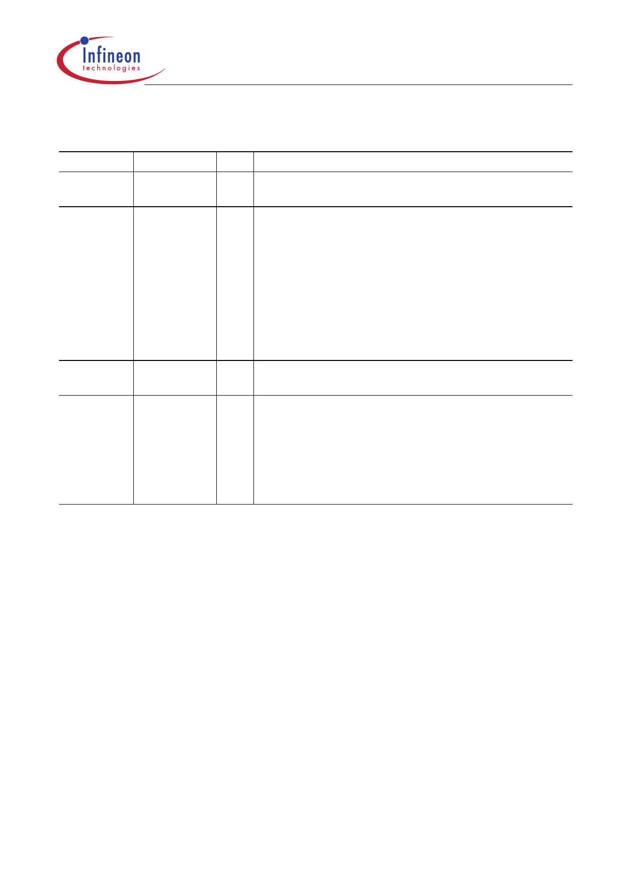
Table 1
Pin Definitions and Functions (cont’d)
Symbol
Pin Number I/O*) Function
XTAL2
47
O XTAL2
Output of the inverting oscillator amplifier.
XTAL1
48
I
XTAL1
Input to the inverting oscillator amplifier and input to the
internal clock generator circuits.
To drive the device from an external clock source, XTAL1
should be driven, while XTAL2 is left unconnected. To
operate above a frequency of 16 MHz, a duty cycle of 50%
should be maintained.
Minimum and maximum high and low times as well as rise/
fall times specified in the AC characteristics (refer to data
Sheet) must be observed.
XTAL4
51
O XTAL4
Output of the inverting real-time clock oscillator amplifier.
XTAL3
52
I
XTAL3
Input to the inverting real-time clock oscillator amplifier.
To drive the real-time clock from an external clock source,
XTAL3 should be driven, while XTAL4 is left unconnected.
Minimum and maximum high and low times as well as rise/
fall times specified in the AC characteristics (refer to Data
sheet) must be observed.
*) I = Input
O = Output
Data Sheet
9
06.99
Share Link: 