NCP1560(2003) データシートの表示(PDF) - ON Semiconductor
部品番号
コンポーネント説明
一致するリスト
NCP1560 Datasheet PDF : 18 Pages
| |||
NCP1560
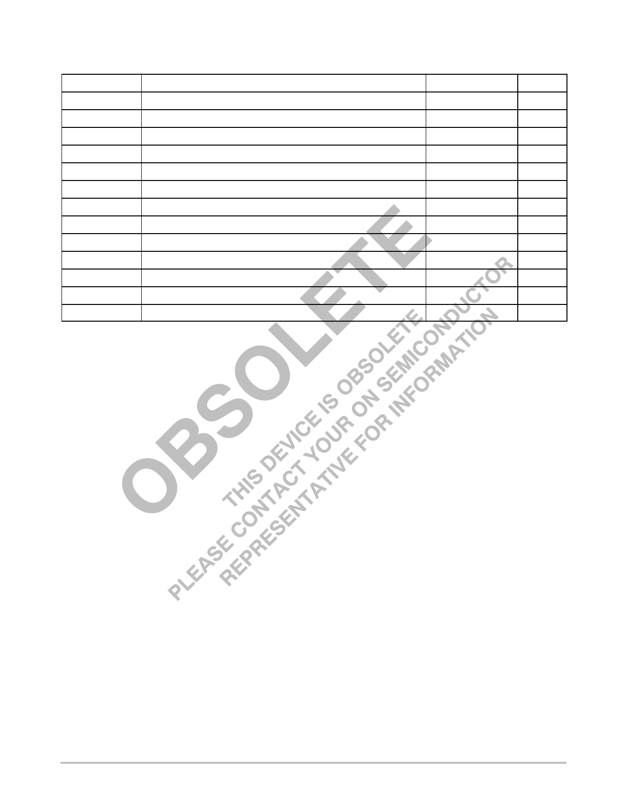
MAXIMUM RATINGS (Note 1)
Rating
Symbol
Value
Unit
Input Line Voltage
Auxiliary Supply Voltage
Auxiliary Supply Input Current
OUT1 and OUT2 Voltage
OUT1 and OUT2 Output Current
5.0 V Reference Voltage
5.0 V Reference Output Current
All Other Inputs/Outputs Voltage
All Other Inputs/Outputs Current
Operating Junction Temperature
Storage Temperature Range
Power Dissipation at TA = 25°C
Thermal Resistance, Junction to Ambient
Vin
VAUX
IAUX
VOUT
IOUT
VREF
IREF
VIO
IIO
TJ
Tstg
PD
RqJA
-0.3 to 150
-0.3 to 16
35
-0.3 to (VAUX + 0.3 V)
10
-0.3 to 6.0
6.0
-0.3 to VREF
10
-40 to 125
-55 to 150
0.77
130
V
V
mA
V
mA
V
mA
V
mA
°C
°C
W
°C/W
1. Maximum Ratings are those values beyond which damage to the device may occur. Exposure to these conditions or conditions beyond those
indicated may adversely affect device reliability. Functional operation under absolute maximum-rated conditions is not implied. Functional
operation should be restricted to the Recommended Operating Conditions.
A. This device series contains ESD protection and exceeds the following tests:
Pin 1 is the HV start-up of the device and is rated to the max rating of the part, or 150 V.
Machine Model Method 150 V.
Pins 2-16: Human Body Model 4000 V per MIL-STD-883, Method 3015.
Machine Model Method 200 V.
http://onsemi.com
5
Share Link: 