NCV8843 データシートの表示(PDF) - ON Semiconductor
部品番号
コンポーネント説明
一致するリスト
NCV8843 Datasheet PDF : 18 Pages
| |||
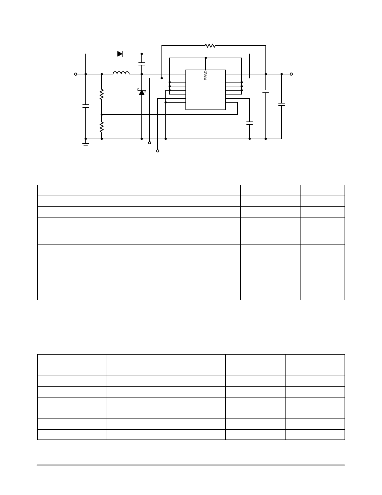
Vout (3.3 V)
D1
L1
18 mH
C1
0.1 mF
R3
D2
162
C3 +
100 mF
R2
100
NCV8843
R6
100k
U1
Vsw
Vin
SHDNB
BOOST
NC
NC
NC
NC
NC
NC
NC
NC
SYNC
Vc
GND
Vfb
NCV8843
C5
0.1 mF
C4
0.1 mF
Vin (7 V to 16 V)
+ C2
330 mF
SHDNB
SYNC
Figure 1. Application Diagram, 7.0 V − 16 V to 3.3 V @ 1.0 A Converter
MAXIMUM RATINGS*
Rating
Value
Unit
Peak Transient Voltage (31 V Load Dump @ VIN = 14 V)
45
V
Operating Junction Temperature Range, TJ
−40 to 150
°C
Lead Temperature Soldering:
Reflow: (Note 1)
260 peak
°C
(Note 2)
Storage Temperature Range, TS
ESD
−65 to +150
°C
(Human Body Model)
2.0
kV
(Machine Model)
200
V
(Charge Device Model)
>1.0
kV
Package Thermal Resistance
SO−16W EPAD Junction−to−Case, RqJC
16
SO−16W EPAD Junction−to−Ambient, RqJA (Note 3)
35
DFN18 Junction−to−Ambient, RqJA (Note 3)
38
SO−8 Junction−to−Ambient, RqJA (Note 4)
100
°C/W
°C/W
°C/W
°C/W
Stresses exceeding those listed in the Maximum Ratings table may damage the device. If any of these limits are exceeded, device functionality
should not be assumed, damage may occur and reliability may be affected.
*The maximum package power dissipation must be observed.
1. 60 second maximum above 183°C.
2. −5°C/0°C allowable conditions.
3. 4 layer board, 1 oz copper outer layers, 0.5 oz copper inner layers, 600 sq mm copper area.
4. 1 in2, 1 oz copper area used for heatsinking.
MAXIMUM RATINGS (Voltages are with respect to GND)
Pin Name
VIN (DC)*
BOOST
VMax
40 V
40 V
VMIN
−0.3 V
−0.3 V
ISOURCE
N/A
N/A
ISINK
4.0 A
100 mA
VSW
VC
SHDNB
40 V
7.0 V
7.0 V
−0.6 V/−1.0 V, t < 50 ns
−0.3 V
−0.3 V
4.0 A
1.0 mA
1.0 mA
10 mA
1.0 mA
1.0 mA
SYNC
7.0 V
−0.3 V
1.0 mA
1.0 mA
VFB
*See table above for load dump.
7.0 V
−0.3 V
1.0 mA
1.0 mA
http://onsemi.com
2
Share Link: 