SM5838AS データシートの表示(PDF) - Nippon Precision Circuits
部品番号
コンポーネント説明
一致するリスト
SM5838AS Datasheet PDF : 14 Pages
| |||
SM5838AS
SPECIFICATIONS
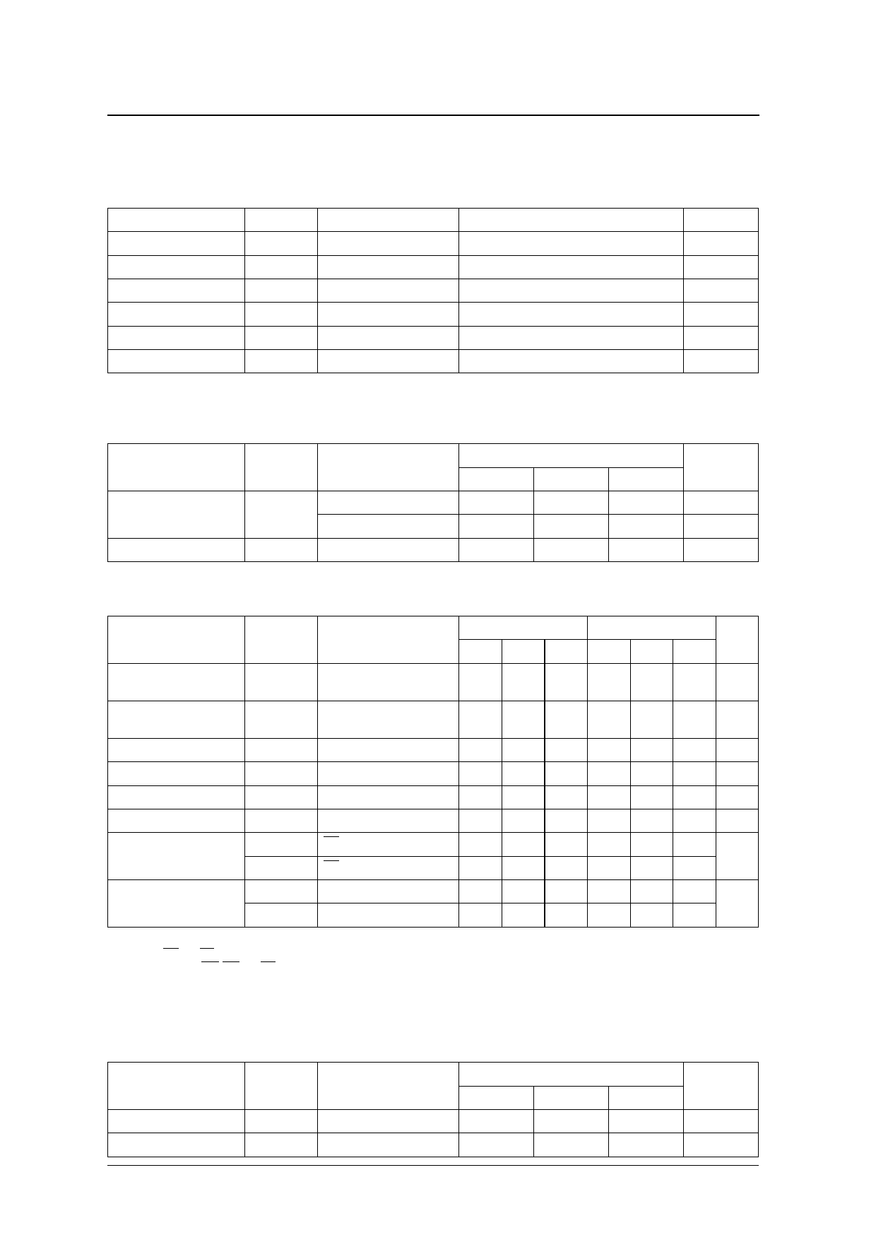
Absolute Maximum Ratings
VSS = 0 V
Parameter
Symbol
Supply voltage range
V DD
Input voltage range
VIN
Storage temperature range
T stg
Power dissipation
PD
Soldering temperature
T sld
Soldering time
tsld
Condition
Rating
Unit
−0.3 to 7.0
V
VSS − 0.3 to VDD + 0.3
V
−40 to 125
°C
500
mW
255
°C
10
s
Recommended Operating Conditions
VSS = 0 V
Parameter
Symbol
Condition
Rating
Unit
min
typ
max
Supply voltage range
Normal-voltage specification
4.5
5.0
5.5
V
V DD
Low-voltage specification
3.0
3.3
4.5
V
Operating temperature
T opr
−20
–
70
°C
DC Characteristics
Parameter
Symbol
Condition
5 V supply
3 V supply
Unit
min typ max min typ max
Operating current
consumption
IDD
No output load1
–
75
90
–
22
30 mA
Standby current
consumption
Input leakage current2
Input leakage current3
Input voltage2
Input voltage3
Output high-impedance
leakage current4
Output voltage4
IST
ILH
VIN = VDD
ILL
VIN = 0 V
V IH
V IL
IZH
OE = HIGH, VOUT = VDD
IZL
OE = HIGH, VOUT = 0 V
V OH
IOH = −1 mA
V OL
IOH = 2 mA
–
–
50
–
–
50
µA
–
–
1
–
–
1
µA
–
–
1
–
–
1
µA
2.4
–
–
2.0
–
–
V
–
–
0.5
–
–
0.5
V
–
–
5
–
–
5
µA
–
–
5
–
–
5
2.5
–
–
2.0
–
–
V
–
–
0.4
–
–
0.8
1. Normal-voltage specification (CLK = 33.3 MHz); Low-voltage specification (CLK = 20 MHz, VDD = 3.3 ± 0.3 V)
2. Pins CLK, RR and RE.
3. Pins DIN0 to DIN7, RW, WE and OE.
4. Pins DOUT0 to DOUT7.
Input/Outputs
Ta = 25°C, f = 1 MHz
Parameter
Input capacitance
Output capacitance
Symbol
CI
CO
Condition
Rating
Unit
min
typ
max
–
–
10
pF
–
–
10
pF
NIPPON PRECISION CIRCUITS—3
Share Link: 