A43L2616V-75I データシートの表示(PDF) - AMIC Technology
部品番号
コンポーネント説明
一致するリスト
A43L2616V-75I Datasheet PDF : 42 Pages
| |||
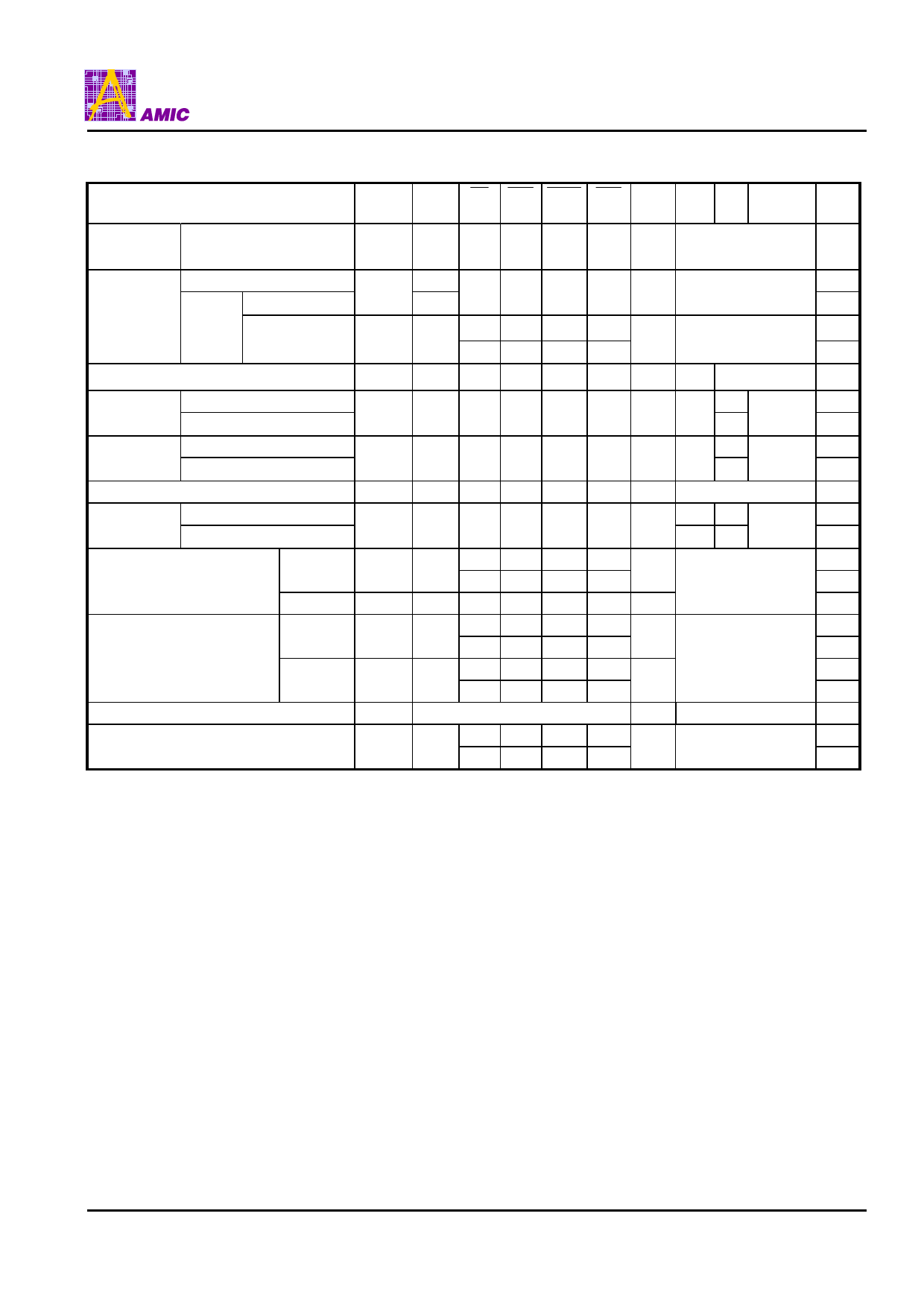
A43L2616B
Simplified Truth Table
Register
Command
Mode Register Set
CKEn-1 CKEn CS RAS CAS WE DQM BA0 A10 A9~A0, Notes
BA1 /AP A11
H
X
LL
L
L
X
OP CODE
1,2
Refresh
Auto Refresh
Self
Refresh
Entry
Exit
Bank Active & Row Addr.
H
3
H
L
L
L
L
H
X
X
3
LHH H
3
L
H
X
X
HX X X
3
H
X
LL
H
H
X V Row Addr.
4
Read &
Auto Precharge Disable
Column Addr. Auto Precharge Enable
L Column 4
H
X
L
H
L
H
X
V H Addr. 4,5
Write &
Auto Precharge Disable
Column Addr. Auto Precharge Enable
L Column 4
H
X
LH
L
L
X
V H Addr. 4,5
Burst Stop
H
X LHH L X
X
Precharge
Bank Selection
Both Banks
VL
H
X
L
L
H
L
X
XH
X
Clock Suspend or
Active Power Down
Entry
H
LHH H
L
X
HX X X
X
Exit
L
H XX X X X
LHH H
Entry
H
L
X
HX X X
Precharge Power Down Mode
X
LVV V
Exit
L
H
X
HX X X
DQM
H
X
V
X
6
No Operation Command
LHH H
H
X
X
X
HX X X
(V = Valid, X = Don’t Care, H = Logic High, L = Logic Low)
Note : 1. OP Code: Operand Code
A0~A11, BA0, BA1: Program keys. (@MRS)
2. MRS can be issued only at both banks precharge state.
A new command can be issued after 2 clock cycle of MRS.
3. Auto refresh functions as same as CBR refresh of DRAM.
The automatical precharge without Row precharge command is meant by “Auto”.
Auto/Self refresh can be issued only at both precharge state.
4. BA0, BA1 : Bank select address.
If both BA1 and BA0 are “Low” at read, write, row active and precharge, bank A is selected.
If both BA1 is “Low” and BA0 is “High” at read, write, row active and precharge, bank B is selected.
If both BA1 is “High” and BA0 is “Low” at read, write, row active and precharge, bank C is selected.
If both BA1 and BA0 are “High” at read, write, row active and precharge, bank D is selected.
If A10/AP is “High” at row precharge, BA1 and BA0 is ignored and all banks are selected.
5. During burst read or write with auto precharge, new read write command cannot be issued.
Another bank read write command can be issued at every burst length.
6. DQM sampled at positive going edge of a CLK masks the data-in at the very CLK (Write DQM latency is 0) but
masks the data-out Hi-Z state after 2 CLK cycles. (Read DQM latency is 2)
(December, 2009, Version 1.3)
8
AMIC Technology, Corp.
Share Link: 